Design
HOW TO DESIGN A PCB LAYOUT
Breadboards are great for prototyping circuits, but they aren’t so good for actually using the thing you’re building. At some point, you’ll probably want to make a project more permanent. The best way to do that is to put it on a PCB.
In this tutorial, I’ll walk you through the process of designing a PCB layout and getting it printed by a custom PCB manufacturer. The performance of your circuit will depend greatly on how it’s laid out on the PCB, so I’ll give you lots of tips on how to optimize your design.
You can always etch PCBs at home with a process that’s similar to developing prints from photographic film. But that method is messy and it uses a lot of chemicals. It’s much easier (and cheaper) to get your PCB made by a professional manufacturer. To demonstrate the process, I’ll use an online service called EasyEDA to design a PCB layout for an LM386 audio amplifier, then I’ll have it manufactured and show you the results. Their free online design software is easy to use and the rates are very affordable.
IT ALL STARTS WITH A SCHEMATIC
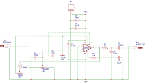
Before you start designing your PCB, it’s a good idea to make a schematic of your circuit. The schematic will serve as a blueprint for laying out the traces and placing the components on the PCB. Plus, the PCB editing software can import all of the components, footprints, and wires into the PCB file, which will make the design process easier (more on this later).
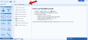
Start by logging in to EasyEDA, and create a new project:

Once you’re on the Start page, click on the “new Schematic” tab:
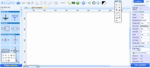
Now you’ll see a blank canvas where you can draw the schematic:
It’s best to place all of your schematic symbols on the canvas before drawing any wires. In EasyEDA, schematic symbols are located in “Libraries”. The default EasyEDA library has most of the common symbols, but there are also “User Generated Libraries” with lots of other symbols:
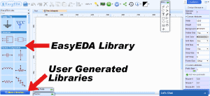
Each schematic symbol you use needs to have a PCB footprint associated with it. The PCB footprint will define the component’s physical dimensions and placement of the copper pads or through holes. Now is a good time to decide which components you’ll be using.
The schematic symbols in the EasyEDA library already have footprints associated with them, but they can be changed if your’re using a different size or style:
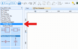
To change the footprint associated with a schematic symbol, search in the “User Generated” libraries for a footprint that matches the component you’re using. Once you find it, click on the heart icon to “Favorite” it:
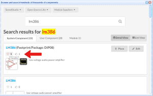
Then copy the name of the component:
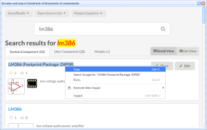
Now click on the symbol in the schematic editor, and paste the name of the new footprint into the “package” field in the right sidebar menu (watch the video below for a demonstration):
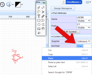
Once all of your symbols are placed on the schematic and you’ve assigned footprints to each symbol, it’s time to start drawing the wires. Rather than explain the details of all that in this article, I’ve made a video so you can watch me draw the schematic for my LM386 audio amplifier:
After all the wiring is done, it’s a good idea to label the symbols. The labels will be transferred over to the PCB layout and eventually be printed on the finished PCB. Each symbol has a name (R1, R2, C1, C2 etc.) and value (10 μF, 100 Ω, etc.) that can be edited by clicking on the label.
The next step is to import the schematic into the PCB editor, but before we do that, let’s talk about some things to keep in mind when designing your PCB.
PCB DESIGN OPTIMIZATION
Identify what each part of your circuit does, and divide the circuit into sections according to function. For example, my LM386 audio amplifier circuit has four main sections: a power supply, an audio input, the LM386, and an audio output. It might help to draw some diagrams at this point to help you visualize the design before you start laying it out.
Keep the components in each section grouped together in the same area of the PCB to keep the conductive traces short. Long traces can pick up electromagnetic radiation from other sources, which can cause interference and noise.
The different sections of your circuit should be arranged so the path of electrical current is as linear as possible. The signals in your circuit should flow in a direct path from one section to another, which will keep the traces shorter.
Each section of the circuit should be supplied power with separate traces of equal length. This is called a star configuration, and it ensures that each section gets an equal supply voltage. If sections are connected in a daisy-chain configuration, the current drawn from sections closer to the supply will create a voltage drop and result in lower voltages at sections further from the supply:

PCB SHAPE AND SIZE
It’s not uncommon to see round, triangular, or other interesting PCB shapes. Most PCBs are designed to be as small as possible, but that’s not necessary if your application doesn’t require it.
If you plan on putting the PCB into an enclosure, the dimensions may be limited by the size of the housing. In that case, you’ll need to know the enclosure’s dimensions before laying out the PCB so that everything fits inside.
The components you use will also have an effect on the size of the finished PCB. For instance, surface mounted components are small and have a low profile, so you’ll be able to make the PCB smaller. Through hole components are larger, but they’re often easier to find and easier to solder.
USER INTERFACES
The location of components like power connections, potentiometers, LEDs, and audio jacks in your finished project will affect how your PCB is laid out. Do you need an LED near a power switch to indicate that it’s on? Or do you need to put a volume potentiometer next to a gain potentiometer? For the best user experience you might have to make some compromises and design the rest of your PCB around the locations of these components.
PCB LAYERS
Larger circuits can be difficult to design on a single layer PCB because it’s hard to route the traces without intersecting one another. You might need to use two copper layers, with traces routed on both sides of the PCB.
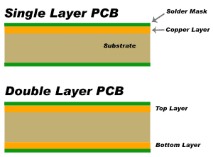
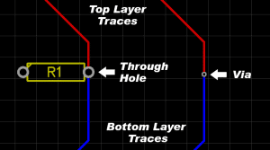
The traces on one layer can be connected to the other layer with a via. A via is a copper plated hole in the PCB that electrically connects the top layer to the bottom layer. You can also connect top and bottom traces at a component’s through hole:
GROUND LAYERS
Some double layer PCBs have a ground layer, where the entire bottom layer is covered with a copper plane connected to ground. The positive traces are routed on top and connections to ground are made with through holes or vias. Ground layers are good for circuits that are prone to interference, because the large area of copper acts as a shield against electromagnetic fields. They also help dissipate the heat generated by the components.
LAYER THICKNESS
Most PCB manufacturers will let you order different layer thicknesses. Copper weight is the term manufacturers use to describe the layer thickness, and it’s measured in ounces. The thickness of a layer will affect how much current can flow through the circuit without damaging the traces. Trace width is another factor that affects how much current can safely flow through the circuit (discussed below). To determine safe values for width and thickness, you need to know the amperage that will flow through the trace in question. Use an online trace width calculator to determine the ideal trace thickness and width for a given amperage.
PCB TRACES
If you look at a professionally designed PCB, you’ll probably notice that most of the copper traces bend at 45° angles. One reason for this is that 45° angles shorten the electrical path between components compared to 90° angles. Another reason is that high speed logic signals can get reflected off the back of the angle, causing interference:
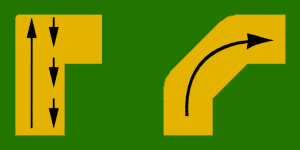
If your project uses digital logic or high speed communication protocols above 200 MHz, you should probably avoid 90° angles and vias in your traces. For slower speed circuits, 90° traces won’t have much of an effect on the performance of your circuit.
TRACE WIDTH
Like layer thickness, the width of your traces will affect how much current can flow through your circuit without damaging the circuit.
The proximity of traces to components and adjacent traces will also determine how wide your traces can be. If you’re designing a small PCB with lots of traces and components, you might need to make the traces narrow for everything to fit.
CREATING THE PCB LAYOUT
Now that we’ve discussed some off the ways you can optimize your PCB design, let’s see how to layout a PCB in EasyEDA.
Open your schematic in the schematic editor, and click on the “Convert Project To PCB” button:
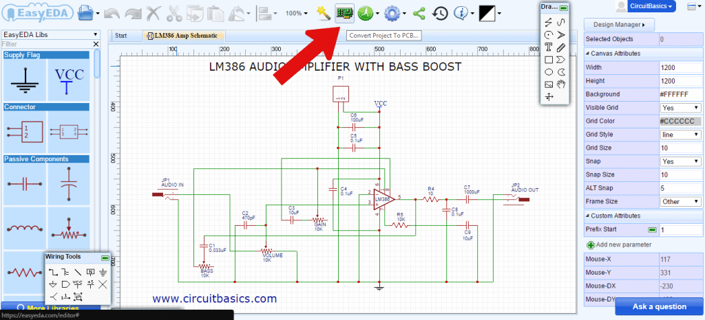
The footprints associated with each schematic symbol will be automatically transferred to the PCB editor:
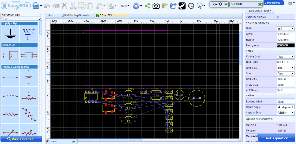
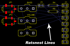
Notice the thin blue lines connecting the components. These are called ratsnest lines. Ratsnest lines are virtual wires that represent the connections between components. They show you where you need to route the traces according to the wiring connections you created in your schematic:
Now you can start arranging the components, keeping in mind the design tips mentioned above. You might want to do some research to find out if there are any special design requirements for your circuit. Some circuits perform better with certain components in specific locations. For example, in an LM386 amplifier circuit the power supply decoupling capacitors need to be placed close to the chip to reduce noise.
After you’ve arranged all of the components, it’s time to start drawing the traces. Use the ratsnest wires as a rough guide for routing each trace. However, they won’t always show you the best way to route the traces, so it’s a good idea to refer back to your schematic to verify the correct connections.
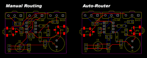
Traces can also be routed automatically using the software’s auto-router. For complicated circuits, it’s generally better to route traces manually, but try the auto-router on simpler designs and see what it comes up with. You can always adjust individual traces later.
This video will show you how to draw traces in EasyEDA’s PCB editor:
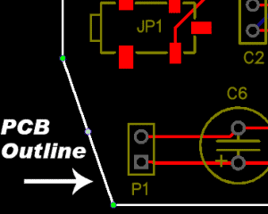
Now it’s time to define the size and shape of the PCB outline. Click on the board outline and drag each side until all of the components are inside:
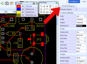
The last thing to do before placing the order is to run a design rule check. A design rule check will tell you if any components overlap or if traces are routed too close together. The design rule check can be found by clicking the “Design Manager” button in the right side window:
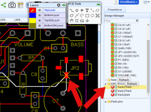
Items that fail the design rule check will be listed below the “DRC Errors” folder. If you click on one of the errors, the problem trace or component will be highlighted in the PCB view:
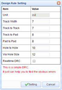
You can specify your own settings for the design rule check by clicking the drop down menu in the upper right hand corner and going to Miscellaneous > Design Rule Settings:
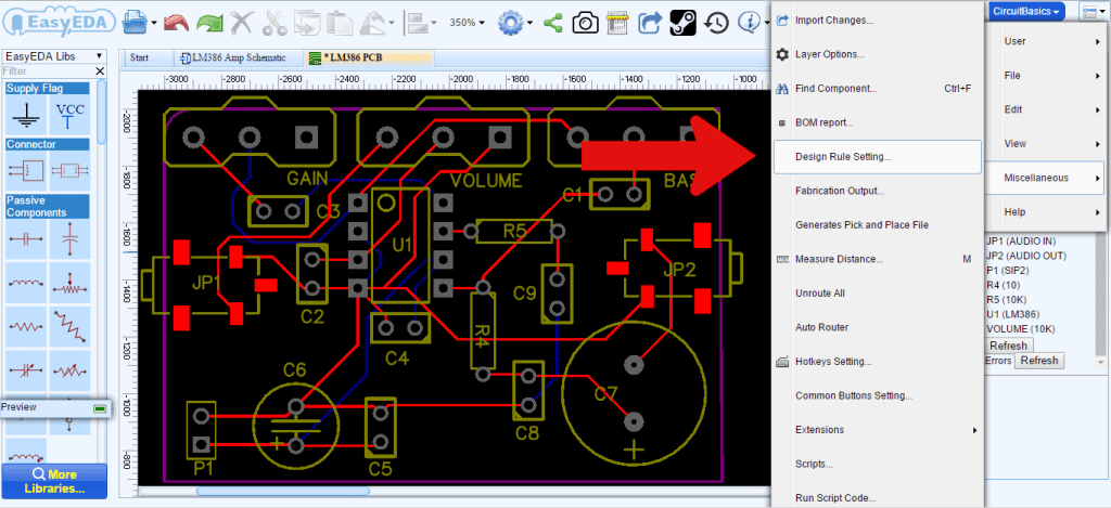
This will bring up a window where you can set design rules for trace width, distance between traces, and other useful parameters:
At this point it’s a good idea to double check your PCB layout against your schematic to make sure that everything is connected properly. If you’re satisfied with the result, the next step is to order the PCB. EasyEDA makes this part really easy…
ORDERING THE PCB
Start by clicking the “Fabrication Output” button in the top menu of the PCB editor:
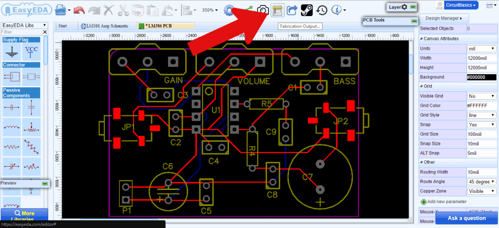
This will take you to another screen where you can choose the options for your PCB order:
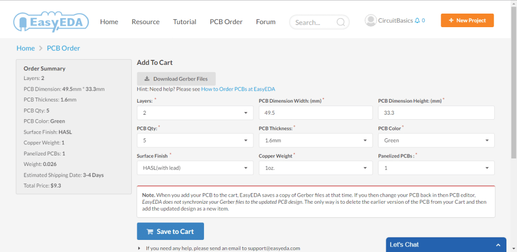
You can select the number of PCBs you want to order, the number of copper layers, the PCB thickness, copper weight, and even the PCB color. After you’ve made your selections, click “Save to Cart” and you’ll be taken to a page where you can enter your shipping address and billing information.
You can also download your PCB’s Gerber files if you want to send them to a different manufacturer:
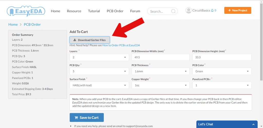
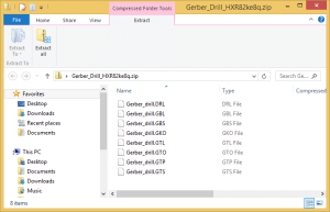
Gerber files are a set of image files that contain the patterns used to manufacture your PCB. All of the files are compressed into a single .zip file. There is a separate file for the copper traces, silk screen, and locations of drill holes and vias:
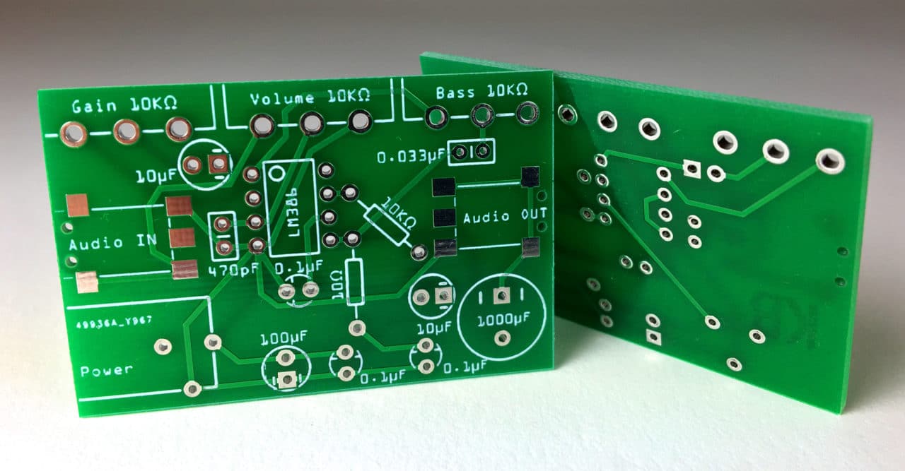
I ordered 15 PCBs for my LM386 audio amplifier circuit and the cost came out to about $15 USD. Manufacturing and shipping took about two weeks. The PCBs were well made, and I couldn’t find any defects. After I soldered on the components and tested the amplifier, it worked great. You can clone my LM386 amplifier schematic and PCB here if you want.
Making your own custom PCB is a lot of fun, and the results can be very rewarding. Hopefully this article will help you get your prototype circuit onto a PCB. Let us know in the comments if you have any questions, and let us know what PCB design projects you have planned. If you liked this tutorial and want to get more like it, be sure to subscribe!

